Crystals used in applications as varied as lasers, LEDs, and the semiconductors in sensors found in astronomical instruments could someday be **‘drawn’ rather than ‘grown’**, leading to higher performance and lower costs.
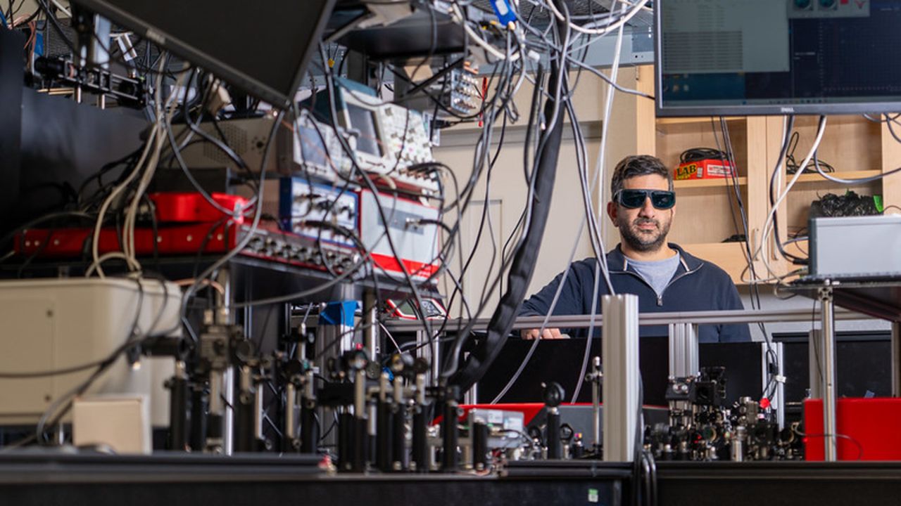
A team led by Elad Harel of Michigan State University has developed an innovative technique that uses a laser to heat a gold nanoparticle, which then triggers crystal formation within a solution of lead halide perovskite. By moving the gold nanoparticle with lasers, it becomes possible—in theory—to precisely **‘draw’ crystals exactly where they are needed** in an electronic device.
### Traditional Crystal Growth: Limitations
Crystals used in electronics are traditionally made through various techniques such as vapor diffusion, where crystals precipitate out of a solution, or by planting a crystal ‘seed’ and allowing it to grow. However, these methods tend to be inaccurate, leading to crystals forming haphazardly and not always in the correct location, shape, or size.
“In a device, one may need a very small quantity of crystalline material placed at very specific locations,” Harel explained to Space.com.
### Plasmonic Heating: A New Level of Control
Harel’s new technique harnesses a phenomenon known as **plasmonic heating** to regain control over crystal formation. In laboratory experiments, his team fired a laser at a wavelength of 660 nanometers onto a gold nanoparticle suspended in a reaction chamber filled with lead halide perovskite precursor solution, layered over a glass substrate made of borosilicate. This substrate is where the crystal is effectively ‘drawn’.
The gold nanoparticle is incredibly tiny—less than one-thousandth the width of a human hair—requiring extreme precision. The entire process can be observed in real time using high-speed microscopes capable of capturing events at sub-millisecond timescales.
“The reason we use gold nanoparticles is because they act as small heaters,” said Harel. “When a laser irradiates the particle at the right frequency, it causes the electrons in the gold to oscillate, which generates heat.”
This **plasmonic heating** drives crystallization of the precursor solution precisely where the researchers want it, allowing for unparalleled accuracy.
### Why Lead Halide Perovskites?
Lead halide perovskite crystals are known for their high performance in devices such as solar cells and LEDs, but they are just one type of crystal used in electronics. For instance, semiconductors on the James Webb Space Telescope’s Mid-Infrared Instrument (MIRI) use arsenic-doped silicon crystals.
Harel hopes that plasmonic heating can be adapted for other crystal types, but it currently works especially well for lead halide perovskites due to their unique properties.
“What’s special about these perovskites is that as the temperature increases, the solubility decreases, which induces crystallization,” Harel explained. “Most materials do not exhibit this retrograde solubility property; typically, solubility increases with temperature.”
Interestingly, the process might involve more than just heat. The excited electrons generated by the laser may also participate directly in the chemistry of crystal formation, encouraging crystal growth beyond thermal effects.
“We do need to do more work to generalize this concept to other materials, but we believe it will work,” Harel added.
### Implications for Industry and Space Exploration
The advantages of this method are clear: **cheaper, faster, and more precise crystal formation** offers significant benefits across many fields. Crystals are ubiquitous in technology—from touchscreens and smoke alarms to solar panels, medical imaging devices, optoelectronics, and photodetectors.
“This is a very simple method using low-cost lasers,” said Harel. “It also saves enormously on the cost of fabrication since the crystal could be placed exactly where and when it is needed.”
Given the importance of crystals in astronomical sensing, this technique could enable the development of **lower-cost instruments for future space missions**.
### The Road Ahead: More Complex Patterns and Real-World Testing
The next step for Harel’s team is to employ multiple lasers across various wavelengths to ‘draw’ more intricate crystal patterns. Following this, the crystals will be tested in real devices to assess whether they deliver superior performance at reduced costs.
“This is something we’re working on right now,” Harel concluded.
—
The ability to ‘draw’ crystals precisely where needed marks a promising leap forward in material science, potentially revolutionizing the manufacture of electronic components and opening new frontiers in both commercial technology and astrophysical research.
https://www.space.com/technology/scientists-discover-new-way-to-grow-materials-on-demand-using-crystals-and-light